or


Results for INVENTOR: ahn kie y. AND FULL_TEXT: {ahn kie y. chappaqua ny}
Showing 1 – 10 of 459
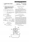
The present invention is directed to a semiconductor interconnect structure comprised of a promoter layer defining openings and a metal layer having a portion elevated above the substrate assembly and a portion that fills the openings. The metal layer is in electrical contact with the substrate assembly through the portion of the metal layer that fills the openings. The portion of the metal layer that fills the openings supports the elevated portion of the metal layer. A method of fabricating a …
 
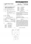
Integrated circuitry and methods of forming integrated circuitry are described. In one aspect, a hole is formed in a semiconductor wafer. In a preferred implementation, the hole extends through the entire wafer. Subsequently, conductive material is formed within the hole and interconnects with integrated circuitry which is formed proximate at least one of a front and back wafer surface. According to one aspect of the invention, integrated circuitry is formed proximate both front and back surface…
 
Integrated circuitry and methods of forming integrated circuitry are described. In one aspect, a hole is formed in a semiconductor wafer. In a preferred implementation, the hole extends through the entire wafer. Subsequently, conductive material is formed within the hole and interconnects with integrated circuitry which is formed proximate at least one of a front and back wafer surface. According to one aspect of the invention, integrated circuitry is formed proximate both front and back surface…
 
An apparatus for forming an electromagnetic field in a processing chamber, including a first pair of electrodes for generating a first electromagnetic field within the processing chamber and a second pair of electrodes for generating a second electromagnetic field within the processing chamber. The first and second pairs of electrodes are oriented so that the first and second electromagnetic fields are oriented generally perpendicular to each other. When energized, the first and second electroma…
 
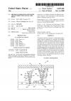
Conductive lines, such as co-axial lines, integrated circuitry incorporating such conductive lines, and methods of forming the same are described. In one aspect, a substrate having an outer surface is provided. A masking material is formed over the outer surface and subsequently patterned to form a conductive line pattern. An inner conductive layer is formed within the conductive line pattern, followed by formation of a dielectric layer thereover and an outer conductive layer over the dielectric…
 
A method for etching materials in which a solid, located in the vicinity of the substrate, is used to provide reactive species for etching the substrate. In contrast with prior art etching techniques, an ion beam is provided which strikes a solid source located in the vicinity of the substrate. Reactive gas species are given off by the solid source when it is hit by the ion beam and these species etch the substrate. Etch rates can be enhanced or retarded depending upon the composition of the sol…
 
The present invention is directed to a semiconductor interconnect structure comprised of a promoter layer defining openings and a metal layer having a portion elevated above the substrate assembly and a portion that fills the openings. The metal layer is in electrical contact with the substrate assembly through the portion of the metal layer that fills the openings. The portion of the metal layer that fills the openings supports the elevated portion of the metal layer. A method of fabricating a …
 
Conductive lines, such as co-axial lines, integrated circuitry incorporating such conductive lines, and methods of forming the same are described. In one aspect, a substrate having an outer surface is provided. A masking material is formed over the outer surface and subsequently patterned to form a conductive line pattern. An inner conductive layer is formed within the conductive line pattern, followed by formation of a dielectric layer thereover and an outer conductive layer over the dielectric…
 
An apparatus for forming an electromagnetic field in a processing chamber, including a first pair of electrodes for generating a first electromagnetic field within the processing chamber and a second pair of electrodes for generating a second electromagnetic field within the processing chamber. The first and second pairs of electrodes are oriented so that the first and second electromagnetic fields are oriented generally perpendicular to each other. When energized, the first and second electroma…
 
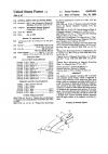
The surface of a magnetic recording disk is encoded with optically sensed indicia, which is employed to control track following of the read/write slider head along a track on a magnetic recording medium such as a disk. The means of reading the medium is to employ a laser carried by the slider which cooperates with the medium as a reflector which affects the lasing function or modulates the operating characteristics of the laser diode. The retro-reflected light changes the operating voltage of th…
 
1 2 3 4 5 6 7 8 9 10
 
 
About |  FAQs |  Terms & Disclaimer |  Link to Us |  Contact Us