or


Results for INVENTOR: hsu sheng teng AND FULL_TEXT: {hsu sheng teng camas wa}
Showing 1 – 10 of 334
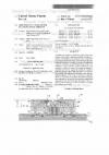
A method of forming a 2/3F pitch high density line array, where F is the minimum line width of a photolithographic process used to accomplish the method of the invention; includes depositing a conductive material on a wafer; depositing a layer of sacrificial material; etching the sacrificial material to form a placeholder having width and space of F; depositing sidewall spacer material hard mask to a thickness of about 1/3F on the sacrificial material; anisotropically etching the hard mask mater…
 
The formation of a fully-depleted, ESD protected CMOS device is described. The device is formed on an SOI or SIMOX substrate, over which an oxide pad is grown to a thickness of between 10 and 30 nm. Appropriate ions are implanted into the oxide to adjust the threshold voltage of an ESD transistor. A portion of the top silicon film is thinned to a thickness no greater than 50 nm. The fully depleted CMOS devices are fabricated onto the thinned top silicon film, while the ESD devices are fabricated…
 
A method of forming, on an ultra-thin SOI substrate, an ESD protected device, includes: preparing a single crystal silicon substrate, including forming insulated areas thereon and forming selectively conductive areas thereon; doping the selectively conductive layers with dopants; growing, epitaxially, silicon layers over selected insulated areas and the doped, selectively conductive areas; heating the substrate and the structures formed thereon at between about 850.degree. C. to 1150.degree. C. …
 
A method of fabricating a ferroelectric memory transistor includes preparing a substrate, including isolating an active region; forming a gate region; depositing an electrode plug in the gate region; depositing an oxide side wall about the electrode plug; implanting ions to form a source region and a drain region; annealing the structure to diffuse the implanted ions; depositing an intermediate oxide layer over the structure; removing the electrode plug; depositing a bottom electrode in place of…
 
A method of forming an electrostatic discharge protected salicided device includes forming, on a single crystal substrate, a source region, a gate channel and a drain region, wherein the source region and drain region are formed by implanting ions of a first type using a low doping density process; depositing a gate oxide layer over the gate channel; masking at least a portion of the drain region and at least a portion of the gate channel and gate oxide layer; implanting ions of a second type to…
 
A method of forming an improved trench isolation structure between transistors on an IC is disclosed. The isolation trench is formed without significantly degrading, or thinning the previously deposited gate oxide layer. The gate oxide layer is deposited on the silicon substrate and covered with a first polysilicon layer. A trench is etched through the first polysilicon layer and gate oxide layer, into the silicon substrate. The edges of the silicon substrate and polysilicon layer, exposed by th…
 
A method of forming an electrostatic discharge protected salicided device includes forming, on a single crystal substrate, a source region, a gate channel and a drain region, wherein the source region and drain region are formed by implanting ions of a first type using a low doping density process; depositing a gate oxide layer over the gate channel; masking at least a portion of the drain region and at least a portion of the gate channel and gate oxide layer; implanting ions of a second type to…
 
A cross-point RRAM memory array includes a word line array having an array of substantially parallel word lines therein and a bit line array having an array of substantially parallel bit lines therein, wherein said bit lines are substantially perpendicular to said word lines, and wherein a cross-point is formed between said word lines and said bit lines. A memory resistor located between said word lines and said bit lines at each cross-point. A high-open-circuit-voltage gain, bit line sensing di…
 
The invention provides a technique for forming a MOS transistor with reduced leakage current and a shorter channel length between source and drain electrodes. The transistor includes a gate electrode between raised source and drain electrodes that are formed from epitaxial silicon. Typically, the raised source and drain electrodes are thin where the intersect the gate electrode so that epitaxial notches are formed between the gate sidewall insulation and the source/drain electrodes. To protect t…
 
The invention provides an improved technique for forming a MOS transistor having lightly doped source and drain junction regions and low parasitic capacitance. The transistor includes raised source and drain electrodes which are strapped to the substrate adjacent the gate insulation. The raised electrodes include interconnect portions which overlie the field oxide separating the semiconductor substrate into a plurality of active regions. The source and drain electrodes are thickest where each ov…
 
1 2 3 4 5 6 7 8 9 10
 
 
About |  FAQs |  Terms & Disclaimer |  Link to Us |  Contact Us