or


Results for INVENTOR: yamazaki shunpei AND FULL_TEXT: {yamazaki shunpei tokyo jp}
Showing 1 – 10 of 1853
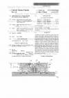
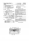
An improved FET is disclosed. The transistor is characterized in that its channel is constituted in the form of a super lattice. The super lattice structure provides a number of square well potential areas through which carriers can pass with little interaction with the gate insulating film.
 
A base member is disposed in a reaction chamber and a raw material gas is introduced thereinto which contains at least a compound gas of a first magnetic material, or the compound gas of the first magnetic material and an oxidizing or nitriding gas, or the compound gas of the first magnetic material and a compound gas of a second magnetic material. A plasma generating electrical energy is applied to the raw material gas to obtain therein a stream of plasma of the raw material gas, by which a str…
 
A semi-amorphous, photoelectric conversion semiconductor which is formed of a mixture of a microcrystalline semiconductor and a non-crystalline semiconductor and in which the mixture is doped with a dangling bond neutralizer, such as hydrogen, chlorine or fluorine, and the microcrystalline semiconductor has a lattice strain and a particle size of 5 to 200 A.
 
A silicon fiber which has a structure expressed by (SiF.sub.2).sub.n where n is greater than 1 and where the fiber may be 1 mm or less in diameter.
 
A silicon fiber which has a structure expressed by (SiF.sub.2).sub.n where n is greater than 1 and where the fiber may be 1 mm or less in diameter.
 
A silicon nitride layer is formed on a substrate by reacting (1) a silicon fluoride, (2) nitrogen or nitrogen hydride and (3) a nitrogen fluoride by a plasma chemical vapor deposition (thermal energy and electronic energy are applied) process. According to the invention, fluorine is added in the silicon nitride layer to produce a Si-F coupling and thus it is made possible to reduce a concentration of hydrogen in the silicon nitride film. It is also possible to make a concentration of oxygen in t…
 
A photoelectric conversion panel which includes a PIN type non-single-crystal semiconductor laminated photoelectric conversion member formed on a substrate, the substrate is formed by a thin, flexible, chemically reinforced glass sheet. A plurality of such photoelectric conversion panels are arranged side by side by means of a flexible plastic frame reinforced with carbon fibers.
 
A manufacturing method of Josephson devices is described. A superconducting ceramic film is deposited on a non-conductive surface and partly spoiled in order to form a barrier film by which two superconducting regions is separated. The spoiling is performed by adding a spoiling element into the ceramic film by ion implantation.
 
An improved semiconductor device manufacturing system and method is shown. In the system, undesirable sputtering effect can be averted by virtue of a combination of an ECR system and a CVD system. Prior to the deposition according to the above combination, a sub-layer can be pre-formed of a substrate in a reaction chamber and transported to another chamber in which deposition is made according to the combination without making contact with air, so that a junction thus formed has good characteris…
 
A semi-amorphous semiconductor device manufacturing method in which a non-single crystal semiconductor layer is provided on a substrate to form therebetween a PN, PIN, PI or NI junction and a current is applied to the non-single crystal semiconductor layer to provide a semi-amorphous semiconductor layer. When the current is applied to the non-single crystal semiconductor layer, it is irradiated by light and/or heated at the same time.
 
1 2 3 4 5 6 7 8 9 10
 
 
About |  FAQs |  Terms & Disclaimer |  Link to Us |  Contact Us