|
Results for ASSIGNEE: kabushiki kaisha toshiba AND FULL_TEXT: {kabushiki kaisha toshiba kawasaki jp}
Showing 1 – 10 of 15842
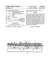
A semiconductor device includes a photodetector for converting an optical signal into an electric signal, and a semiconductor element comprising an optical transmissible conductive film formed through an insulating film on the main surface of a semiconductor with a photodetector, and electrically connected to a constant potential line of the semiconductor device, a wiring layer formed through an insulating film on the main surface of the semiconductor formed with the semiconductor element, an in…
An electrode device including an insulating body, at least one conductor mounted on the insulating body, and an insulating member mounted on the conductor and supporting high voltage slip-ring electrodes to which high voltages are applied.
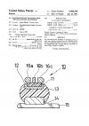
In a sputtering target supporting device for fixing, to a common electrode, a plurality of beams forming a mosaic target used for co-sputtering, at least one pressing mechanism is provided exclusively for each of the beams to press the respective beam against the common electrode by means of the respective pressing mechanism provided therefor.
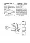
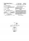
In a distributed processing system having a plurality of nodes, a correspondence table, which represents a correspondence between the nodes and corresponding passwords that grant access to the nodes, stored in a disk device. Each of the nodes includes a passthrough device which permits passthrough of access request data to a node of the next hierarchical level. Upon receipt of access request data, the passthrough device refers to the correspondence table to check a password contained in the rece…
A pointing apparatus includes a direction determination circuit for determining a moving direction of a cursor in accordance with cursor current position information and cursor moving information input from a mouth, and a cursor jump circuit for recognizing the presence/absence of an icon to be designated by the cursor near a position along the moving direction determined by the direction determination circuit, and for jumping the cursor to the position of the icon.
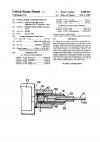
An optical circuit device includes an optical fiber element, a lens and several holders. An inner holder which is elastic, holds the optical fiber element and a lens on the same optical axis. An intermediate holder fixes the inner holder therein. An outer holder, which is connected to an optical signal receiving device, holds the intermediate holder therein. An optical axis of the inner holder is adjusted by shifting the position of the intermediate holder in the outer holder parallel to the opt…
An X-ray imaging apparatus comprises an X-ray generator, an image intensifier for converting an X-ray image of a subject under examination to an optical image, a solid state image sensor for picking up the optical image of the image intensifier, a driver circuit for driving the solid state image sensor and a television monitor for visually displaying an image signal obtained from the solid state image sensor as an X-ray optical image. The X-ray generator is controlled such that an X-ray pulse is…
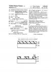
In a patterning method according to this invention, a surface region of a resist layer is solution-retarded by a developer, and, then, the resist layer is patterned. Therefore, a desired shape of a side wall of the resist layer may be obtained by varying a solubility of the resist layer, with the result that a resist pattern with the side wall orthogonal to a surface of the substrate or the overhung side may be formed.
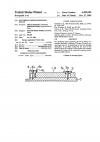
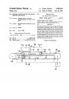
An optical scanning device for an image forming apparatus includes a document table on which an original document is placed, an image carrier, and a carriage for transmitting reflected light from the original document onto the image carrier. The optical scanning device further includes a pair of guide rails for supporting the carriage and for guiding movement of the carriage, a moving mechanism for moving the carriage in a prescribed direction along the guide rails, and a pair of holding rollers…
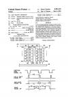
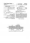
First conductive members are buried in first holes formed in a first insulating film to connect the second interconnection layers, formed through first and second insulating films, to a semiconductor substrate. Second conductive members are buried in second holes formed to be positioned on the first holes of the second insulating film. Thus, the reliability of a semiconductor device of a multi-layer interconnection structure is improved, and the integration thereof is improved.
|

|