or


Results for ASSIGNEE: seiko epson corporation AND FULL_TEXT: {seiko epson corporation tokyo jp}
Showing 1 – 10 of 9074
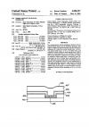
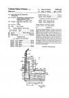
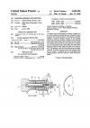
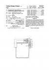
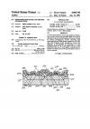
A novel semiconductor device and method of production of such a device are provided. Both the N and P channels of the novel semiconductor device are formed by contact self-alignment, thereby permitting high speed operation and high density integration to be realized. The formation of the channels by contact self-alignment is accomplished by depositing a P type polysilicon layer on an N well region and an N type polysilicon layer on a P well region. A silicide layer if formed over both the P and …
 
In a semiconductor device including a substrate of Si or polycrystalline silicon and an interlayer insulation film region, a region for interconnection with the substrate is composed of a refractory metal silicide layer, a refractory metal nitride layer, an Al or Al alloy layer, and possibly a further refractory metal nitride layer, while a region for interconnection on the interlayer insulation film on the substrate is composed of a refractory metal, or refractory metal oxide layer, a refractor…
 
A printer for receiving print instructions from one of a plurality of host units includes an input data storage unit for storing the data including control codes and character codes input by the selected host unit. At least two print control units having internal character code/control code groups process the data in the input data storage unit in accordance with the internal control codes. A character code/control code judging unit decodes the plurality of character codes/control code groups st…
 
A projection-type display device using twisted nematic liquid crystal light valves in which the photoelectric transfer characteristics of three light valves for selectively transmitting red, green and blue light to a synthesizing device are matched. The product of the birefrigence .DELTA.n and thickness d of the twisted nematic liquid crystal and thickness of cell is selected to fall within a predetermined optimal range of values depending upon the wavelength of light which travels therethrough….
 
A wire dot printer includes a print head which is more reliable and better controls a gap between a magnetic pole and a print lever. The print head includes a core block and nose block. The core block includes a projection for regulating oscillations of a print lever at its inner central portion. A print lever drive coil for each print lever is formed on the core block about the projection. The nose block includes a disk member which is mounted opposed to the core block. A print lever is movably…
 
An ink jet printing apparatus in which the ink jet print head is constructed to eliminate problems caused by air bubbles that can be present in fluid hot-melt ink. The apparatus head includes a heater to melt solid ink or lower the viscosity of high viscosity semi-solid ink and a plurality of ink jet nozzles corresponding to a series of piezoelectric vibrating elements that are positioned so that piezoelectric oscillations propel ink through the nozzles. The vibrators and nozzles are spaced so t…
 
The approaching end of usable ink ribbon which is being supplied from a cassette to a serial printer is signaled when a detector member which rides on used ink ribbon as it is wound onto the take-up spool of the cassette, reaches a predetermined distance away from the axis of the take-up spool and moves to project through an opening in the cassette. The wall of the cassette serves as a barrier to motion of the detecting member, with the opening in the wall establishing the predetermined diameter…
 
A plunger type electromagnetic hammer assembly for use with a printer including a hammer housing having a magnetic flux emitting surface. The hammer assembly includes a hammer slidably situated in the housing wherein the hammer includes a plunger portion having a first radius and a head portion having a second radius. The plunger portion and the head portion are coupled by a neck portion having a third radius, the third radius being less than the first radius and than the second radius. The plun…
 
A chiral phenylether compound having the formula ##STR1## wherein X is a halogen atom; m is an integer from 3 to 5, n is an integer from 3 to 12 and * designates an asymmetric carbon is disclosed. The chiral phenylether compounds are useful to prepare chiral smectic phase pyrimidine phenylether liquid crystal compounds of the formula. ##STR2## The reaction is carried by reacting (I) with butylithium, dissolving in ether and reacting with a 1-bromoalkane to yield (IV). Compounds (IV) are particul…
 
A construction for removing electrical charge generated in a data input device when the data input device is connected to a data storage device. Contacting members connected to a ground are provided on the connector of the electronic apparatus and contact conductive members of the input device to remove electrical charges prior to connecting the input terminals of the input device to the connector terminals of the electronic apparatus.
 
1 2 3 4 5 6 7 8 9 10
 
 
About |  FAQs |  Terms & Disclaimer |  Link to Us |  Contact Us