or


Results for ASSIGNEE: sharp kabushiki kaisha AND FULL_TEXT: {sharp kabushiki kaisha osaka jp}
Showing 1 – 10 of 11140
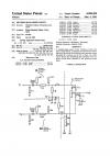
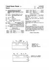
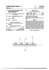
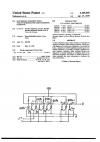
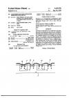
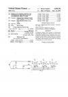
A brilliance control circuit capable of automatically controlling the brilliance of fluorescent display tubes, comprising a lighting voltage regulating circuit incorporating a circuit element which decreases the lighting voltage when the current flowing through the fluorescent display tube increases, and increases the lighting voltage when the current decreases.
 
A contact pin comprising an end tip which is to be brought into contact with a terminal disposed of an IC card, for the transmission of an electric signal through the terminal, the end tip consists of an elastic body which is electrically conductive so that the terminal is prevented from being damaged while assuring the electrical contact between the end tip and the terminal.
 
A liquid crystal display element for matrix display, employing, as address elements, thin film transistors each having a layered arrangement of a gate electrode, an insulating film, a semiconductor film, a source electrode, a drain electrode and a display picture element electrode formed in that order on an insulating substrate. The liquid crystal display element is characterized by a thin metallic film for smoothing path lines for the source electrodes, formed of the same material as that formi…
 
A multiple-band mixer circuit includes at least two mixer circuit blocks, a selection circuit block for selecting one of the mixer circuit blocks, and a monitor circuit provided for common use by the at least two mixer circuit blocks, for monitoring the operation state of a mixer circuit block selected by the selection circuit block.
 
In a reflective type liquid crystal display comprising a rear support plate carrying segmented reflective electrodes in a predetermined display region, a front transparent support plate carries first and second reflective coatings in a region except the region corresponding to said segmented reflective electrodes, and a transparent electrode is deposited on said front support plate and said second reflective coating. An intermediate layer of insulator material is interposed between said first an…
 
A pair of metal rollers to which a predetermined pressure is applied are provided in an electrophotographic copying machine for fixing a developed image carried on a copy paper driven to travel through said pair of metal rollers. At least one of said rollers is slightly inclined with respect to a line perpendicular to a transportation direction of the copy paper in order to stabilize the fixing operation. In a preferred form, both of said rollers are slightly inclined in counter directions to ea…
 
During the manufacture of an I.sup.2 L device, to achieve diffusion steps for a collector region and a collar region at the same time, polycrystal silicon is deposited over the whole surface of the collector region and then an impurity is diffused simultaneously into the collector region and the collar region.
 
A plurality of solar cell elements are arranged on a supporting substrate. Each solar cell element has a light receiving surface, where electrodes are formed which are connected to the P-type region and the N-type region contained within the solar cell element, respectively. The electrodes formed on the light receiving surfaces of the plural solar cell elements are electrically connected to each other by light transmitting, electrically conductive wiring means formed on the light receiving surfa…
 
A time calculation ring counter is made of a plurality of negative resistance light emitting elements, which provide display of current time information. In a preferred form, a plurality of GCR’s (gallium arsenide gate controlled rectifiers) or a plurality of GND’s (gallium arsenide negative resistance light emitting diodes) are aligned in a circular fashion on a display panel of an electronic timepiece. The GCR’s or GND’s function to either calculate the time information or indicate the time in…
 
Formation of well-regions of a conductivity type opposite to that of a substrate is achieved in such a manner to determine a first threshold voltage level. Ion implantation is effected on desirably selected gates in the respective channels formed on the substrate and the well-regions. Two channels on the ion implanted substrate and on the well-region in which the ion implantation is not effected, are coupled to form a complementary-MOS transistor pair having a first threshold voltage level. The …
 
1 2 3 4 5 6 7 8 9 10
 
 
About |  FAQs |  Terms & Disclaimer |  Link to Us |  Contact Us