or


Results for ASSIGNEE: fujitsu limited AND FULL_TEXT: {fujitsu limited kawasaki jp}
Showing 1 – 10 of 18734
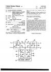
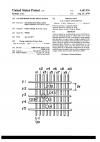
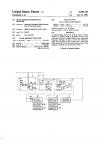
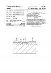
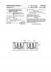
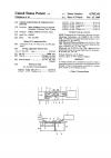
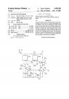
A semiconductor memory includes memory cells and a discharge current source for quickly discharging electric charges, in the form of a discharge current, stored along the word lines. Each of the memory cells is comprised of a load transistor pair and a multi-emitter type detection transistor pair. The discharge current source controls the discharge current by means of a bias circuit formed in the discharge current source. The bias circuit control the value of the discharge current in accordance …
 
A microwave signal amplifier comprising transistor having input and output terminals further includes input and output matching circuits connected to the input and output terminals, respectively, and corresponding bias supply circuits connected in parallel between said transistor and said input and output matching circuits, respectively. The input and output matching circuits are each implemented by high pass filters, and the bias supply circuits are each implemented by low pass filters. Further…
 
A drive system for an alternating current (AC) driven type gas discharge panel in which either one of the electrode pitches of X and Y electrodes is made smaller than the other. A positive pulse voltage is applied to the electrodes of the smaller electrode pitch and a negative pulse voltage is applied to the electrodes of the larger electrode pitch, thereby to write information in a selected discharge point. The AC driven type gas discharge panel of an electrode arrangement of an asymmetrical el…
 
A quick feeding system for feeding quick counting pulses to a counter, such as an hours counter of an electronic clock of the digital display type, comprising frequency dividing circuits, a switch for effecting a quick feed of pulses to the counter and a quick feed pulse generation circuit connected between one of the frequency dividing circuits and the counter.
 
A compound semiconductor device comprises: a III-V group compound semiconductor substrate and a Schottky junction electrode of p-type amorphous silicon carbide (a-SiC) layer provided on the III-V group compound semiconductor substrate and an amorphous silicon-germanium-boron (a-Si-Ge-B) layer provided on the p-type amorphous silicon carbide layer.
 
A low dielectric constant ceramic substrate comprised of 90 to 98% of mullite (3Al.sub.2 O.sub.3. 2SiO.sub.2) and 10 to 2% of a sintering promotor comprised of 0.5 to 3% of magnesia (MgO) and 1.5 to 7% of calcium oxide (CaO).
 
A semiconductor device includes trench capacitors formed in a semiconductor substrate, a trench provided therebetween for isolating the trench capacitors, and a trench capacitor formed in a side wall of the trench for isolating the trench capacitors.
 
A wiring structure for a termination circuit in which a termination circuit is connected to an integrated circuit through a fixed wiring pattern provided in a leadout layer closest to the mounting surface.
 
An optical fiber connector structure for minimizing loss in an optical fiber connector. The connector includes cylindrical member for housing ferrule, a C-ring having a pawl positioned about the cylindrical member, and grooves formed in the cylindrical member for engaging the pawl so that the plug can engage the adapter so as to minimize loss in the connection with minimal amount of adjustment.
 
A method for fabricating a semiconductor device comprises forming a contact hole in an insulating film formed on a first wiring composed of an Al film, covering the insulating film with an Al film for a second wiring, applying laser beam pulses to the Al film for a second wiring from above, and patterning the Al film to form a second wiring.
 
1 2 3 4 5 6 7 8 9 10
 
 
About |  FAQs |  Terms & Disclaimer |  Link to Us |  Contact Us