or


Results for ASSIGNEE: intel corporation AND FULL_TEXT: {intel corporation santa clara ca}
Showing 1 – 10 of 17738
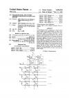
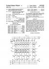
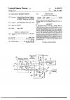
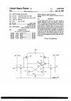
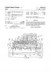
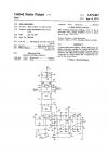
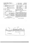
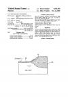
A process for growing field oxide regions in an MOS circuit. An initial thermally grown layer of silicon nitride seals the substrate surface and reduces lateral oxidation, or bird’s beak formation along the substrate-nitride interface. Field oxidation takes place in two steps, with the first step being a dry oxidation in HCL and the second taking place in steam.
 
A semiconductor cell for producing an output current that is related to the match between an input vector pattern and a weighting pattern is described. The cell is particularly useful as a synapse cell within a neural network to perform pattern recognition tasks. The cell includes a pair of input lines for receiving a differential input vector element value and a pair of output lines for providing a difference current to a current summing neural amplifier. A plurality of floating gate devices ea…
 
A virtual ground electrically programmable read-only memory device in which disturbance to neighboring cells is practically eliminated, is disclosed. In one embodiment the memory device comprises a plurality of memory cells formed in a semiconductor substrate and arranged in rows and columns so as to form an array. During read operations, pairs of adjacent cells are accessed simultaneously by grounding a single column line within the array. The two adjacent column lines–one on each side of the …
 
A redundant memory circuit for a memory array in which the memory has a preselected number of rows and columns having addresses associated therewith and decoders coupled thereto and one or more redundant rows or columns having initially unspecified addresses associated therewith and redundant decoders coupled thereto. The redundant memory circuit programs the redundant decoders coupled to the redundant rows or columns having initially unspecified addresses to match the addresses of defective row…
 
A non-volatile MOS memory cell which includes a bistable (flip-flop) circuit with slightly imbalanced loads. An electrically programmable, floating gate device is coupled across a portion of one of the loads to permit selective shunting. When the cell is powered-down (such as at power failure), the floating gate is either charged or discharged as a function of the state of the flip-flop. When power is reapplied, the imbalance caused by the selective shunting forces the flip-flop to its previous …
 
A gas reactor for depositing thin films such as silicon dioxide, the lid of the reactor includes a plurality of concentric rings and a plurality of ports disposed between adjacent rings, a generally radial flow above the specimens is maintained in the reactor.
 
In connection with the fabrication of an integrated circuit, a method for simultaneously completing the formation of a contact, an interconnect, a gate and a source or drain is disclosed. An integrated circuit field effect structure wherein a diffused silicon area is connected directly to a polysilicon member by conductive silicon and more specifically the source or drain of one device is directly and continuously connected to the gate of an adjacent device by a conductive silicon member.
 
A metal-oxide-semiconductor (MOS) differential amplifier particularly suitable for sensing the state of a memory cell, which includes a pair of column lines, is disclosed. The differential amplifier is biased such that it operates in a linear region and is capacitively coupled to the column lines.
 
A capacitor-like MOS structure which provides a fusible link useful in a ROM, redundancy circuit, or the like is disclosed. An oxide layer insulates a polysilicon electrode from a doped substrate region. A potential is applied between the electrode and the doped region of sufficient magnitude to cause the oxide to rupture and to cause permanent filaments to be formed within the oxide. The filaments provide permanent conductive links between the polysilicon electrode and the doped substrate regio…
 
A synchronous delay line with quadrature clock phases provides for an improved output from the taps of a delay line. The delay line is comprised of a phase generator, a plurality of voltage controlled delay stages arranged serially, wherein the last VCD stage is coupled to a sample-and-hold circuit for providing an analog control voltage for controlling the delay. The phase generator generates in-phase clock signals to the interior delay stages, but provides quadrature clock phases to the delay …
 
1 2 3 4 5 6 7 8 9 10
 
 
About |  FAQs |  Terms & Disclaimer |  Link to Us |  Contact Us