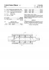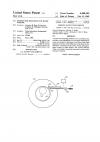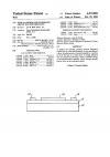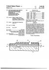


A transparent conductive layer of SnO.sub.2 is deposited on a substrate by an RF-plasma assisted chemical vapor reaction of CO.sub.2 with an organic tin compound, such as tetramethyl tin, for example. A CCD optical imager is fabricated, using the method of the invention to form a transparent conductive layer thereon.