or


Results for INVENTOR: gardner mark i. AND FULL_TEXT: {gardner mark i. cedar creek tx}
Showing 1 – 10 of 490
The formation of lightly doped regions under a gate of a transistor via gate autodoping is disclosed. One embodiment of the invention is a method having four steps. In the first step, a gate having two sidewalls is provided over a gate oxide over a semiconductor substrate; source and drain regions with the substrate adjacent to the sidewalls of the gate are also provided. In the second step, the gate oxide is etched to reduce the length of the gate oxide. In the third step, a spacer is formed at…
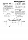
 
A semiconductor device having an nitrogen-rich punchthrough region under the channel region, and a process for fabricating such a device are disclosed. In accordance with one embodiment, a semiconductor device is formed by forming an nitrogen-rich punchthrough region in a substrate, and forming a channel region over the nitrogen-rich punchthrough region. The use of an nitrogen-rich punchthrough region may, for example, inhibit the diffusion of dopants used in forming the channel region.
 
A method of doping a semiconductor substrate with a single masking step. A semiconductor substrate having a first region and a laterally displaced second region is provided. A patterned masking layer is then formed on an upper surface of the semiconductor substrate over the first region. A first well impurity distribution is then formed in the semiconductor substrate such that a peak concentration of the first well impurity distribution is located at a first well depth below the upper surface in…
 
A semiconductor device fabrication process in which an active region of a semiconductor device is formed by diffusing a dopant out of a sidewall spacer. According to the process, a gate electrode is formed on a substrate and an active region of the substrate adjacent the gate electrode is doped with a first dopant of a first conductivity type to form a heavily-doped region in the active region. A spacer layer having a second dopant disposed therein is then formed. The second dopant has a second …
 
A semiconductor fabrication process in which a transistor trench and an isolation trench are simultaneously formed in a semiconductor substrate. The transistor trench is laterally displaced from the isolation trench. Thereafter the isolation trench is filled with an isolation material and a gate dielectric is formed on the floor of the transistor trench. Next, a conductive gate is formed on the gate dielectric and a source/drain impurity distribution is introduced into a source region and a drai…
 
A semiconductor device having a nitrogen-bearing gate electrode and method of fabricating the same is provided. Consistent with the invention, a semiconductor device is formed by forming a gate oxide layer on a surface of a substrate. Over the gate oxide layer is formed a lower polysilicon layer with a first nitrogen concentration. Over the lower polysilicon layer, there is formed an upper polysilicon layer with a second nitrogen concentration less than the first nitrogen concentration. The two …
 
A method and structure are provided for an IGFET which has a replaceable gate electrode fabrication and dual polished fabrication technique to simultaneously form source, drain and gate regions. The IGFET provides a raised metal layer between the source/drain areas and subsequent metallization layers. The IGFET provides a second gate material formed from a refractory metal which creates a gate junction with low contact resistivity. The refractory metal gate and the metal layer are formed over th…
 
A semiconductor manufacturing process for producing MOS integrated circuits having two gate oxide thickness is provided. A first gate dielectric is formed on an upper surface of a semiconductor substrate. Thereafter, a masking layer is deposited on the first dielectric layer and patterned such that the first dielectric layer is exposed above a second region of the semiconductor substrate. The semiconductor wafer is then subjected to a thermal oxidation process such that a second gate dielectric …
 
A semiconductor fabrication process in which a transistor trench and an isolation trench are simultaneously formed in a semiconductor substrate. The transistor trench is laterally displaced from the isolation trench. Thereafter the isolation trench is filled with an isolation material and a gate dielectric is formed on the floor of the transistor trench. Next, a conductive gate is formed on the gate dielectric and a source/drain impurity distribution is introduced into a source region and a drai…
 
An integrated circuit fabrication process is provided for forming a transistor in which the source/drain areas are formed simultaneously with the lightly doped drain areas. A gate electrode including a high-K gate dielectric and a gate conductor is formed upon a semiconductor substrate. The high-K gate dielectric is then selectively narrowed relative to the gate conductor. The source/drain areas and lightly doped drain areas are formed using a single impurity implant without the need for sidewal…
 
1 2 3 4 5 6 7 8 9 10
 
 
About |  FAQs |  Terms & Disclaimer |  Link to Us |  Contact Us