or


Results for INVENTOR: takemura yasuhiko AND FULL_TEXT: {takemura yasuhiko kanagawa jp}
Showing 1 – 10 of 295
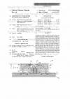
Superconducting oxide ceramics having a high density of superconducting current are formed without making use of very high temperatures higher than 1000.degree. C. Superconducting oxide material is placed in a crucible, melted and fired at a relatively low temperature. During the melting and firing step, the partial pressure of oxygen is reduced in order to lower the melting point of the ceramic. After the firing, the partial pressure of oxygen is increased.
 
A new type of superconducting memory is described. The composition of superconducting ceramic material used in the memory has been altered in order to expedite the formation of non-superconducting regions formed of grain boundaries. Non-superconducting regions may also be formed of lattice defects. Magnetic flux is trapped within the non-superconducting regions (grain boundaries or lattice defects). Information can be stored in terms of whether or not magnetic flux is trapped.
 
An electro-optical liquid crystal display suitable for displaying highly graded images. A plurality of pixels are arranged in a matrix and supplied with data signals through data lines extending in the column direction. Extending in the row direction are a plurality of addressing lines and a plurality of voltage signal lines. Each row is selected by activating by each of the addressing lines and supplied with a driving voltage from each of the voltage supplying lines.
 
Two kinds of TFTs are fabricated by the same process with a high production yield to manufacture an active-matrix circuit and a peripheral driver circuit on the same substrate. The active-matrix circuit is required to have a high mobility and a high ON/OFF current ratio. The peripheral driver circuit needs a complex interconnection structure. The active-matrix circuit and the peripheral driver circuit comprising the TFTs are fabricated monolithically. In this step, the gate electrodes of the TFT…
 
A thin film transistor of reversed stagger type having improved characteristics and yet obtained by a simple process, which is fabricated by selectively doping the semiconductor region on the gate dielectric to form the source, drain, and channel forming regions by using ion implantation, ion doping, or doping a plasma of ions; and then effecting rapid thermal annealing by irradiating a ultraviolet radiation, a visible light, or a near-infrared radiation for a short period of time. The source, d…
 
A process of operating an active matrix display device having thin film transistors by supplying an address signal to a gate of a first thin film transistor so the first thin film transistor is in an ON state, by applying a data signal to one of a pair of impurity regions of the first thin film transistor when the first thin film is in the ON state, supplying said data signal to a gate of a second thin film transistor through the first thin film transistor, and by applying a voltage to one of a …
 
An active matrix display device for suppressing voltage variation .DELTA.V due to off-operation of a gate pulse, including TFTs and picture-element electrodes, at least one of the TFTs being assigned to each picture element, and each of the TFTs having a gate electrode connected to a gate line (first gate line), and a source and a drain one of which is connected to a data line, wherein a picture-element electrode concerned is formed so as to be overlapped with the first gate line through an insu…
 
A halogen fluoride such as ClF.sub.3 is introduced into the chamber of the doping system. During the doping process, boron adhering to the inner wall of the chamber is changed into gaseous boron fluoride (such as BF.sub.3) and driven off.
 
A semiconductor device having a substrate having an insulating surface; at least first and second semiconductor islands formed over the substrate where each of the semiconductor islands has a channel region and a pair of impurity regions; an insulating film formed over the substrate, the insulating film including at least first and second gate insulating films formed over the first and second semiconductor islands, respectively; at least first and second gate electrodes formed over the first and…
 
An active matrix display device for suppressing voltage variation .DELTA.V due to off-operation of a gate pulse, including TFTs and picture-element electrodes, at least one of the TFTs being assigned to each picture element, and each of the TFTs having a gate electrode connected to a gate line (first gate line), and a source and a drain one of which is connected to a data line, wherein a picture-element electrode concerned is formed so as to be overlapped with the first gate line through an insu…
 
1 2 3 4 5 6 7 8 9 10
 
 
About |  FAQs |  Terms & Disclaimer |  Link to Us |  Contact Us