or


Results for INVENTOR: wood alan g. AND FULL_TEXT: {wood alan g. boise id}
Showing 1 – 10 of 333
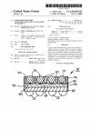
A semiconductor component includes a carrier and multiple semiconductor substrates stacked and interconnected on the carrier. The carrier includes conductive members bonded to corresponding conductive openings on the semiconductor substrates. The component can also include terminal contacts on the carrier in electrical communication with the conductive members, and an outer member for protecting the semiconductor substrates. A method for fabricating the component includes the steps of providing …
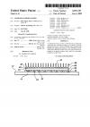
 
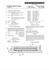
A condensed memory matrix is fabricated by conductively connecting the attachment bumps of a substrate with the attachment bumps of a wafer of DRAM chips and physically bonding the juxtaposed surfaces of the substrate and the wafer with a dielectric curable resin. An array of heat fins is bonded to the inactive surface of the wafer by a thermally conductive curable resin.
 
A condensed memory matrix is fabricated by conductively connecting the attachment bumps of a substrate with the attachment bumps of a wafer of DRAM chips and physically bonding the juxtaposed surfaces of the substrate and the wafer with a dielectric curable resin. An array of heat fins is bonded to the inactive surface of the wafer by a thermally conductive curable resin.
 
A condensed memory matrix is fabricated by conductively connecting the attachment bumps of a substrate with the attachment bumps of a wafer of DRAM chips and physically bonding the juxtaposed surfaces of the substrate and the wafer with a dielectric curable resin. An array of heat fins is bonded to the inactive surface of the wafer by a thermally conductive curable resin.
 
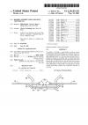
A center bond flip-chip device carrier and a method for making and using it are described. The carrier includes a flexible substrate supporting a layer of conductive material and a layer of elastomeric material. At least one pocket is formed in the layer of elastomeric material and sized and shaped to house a solder ball. The solder ball is electrically connected to a die positioned on the layer of elastomeric material and also electrically connected to the layer of conductive material.
 
A condensed memory matrix is fabricated by conductively connecting the attachment bumps of a substrate with the attachment bumps of a wafer of DRAM chips and physically bonding the juxtaposed surfaces of the substrate and the wafer with a dielectric curable resin. An array of heat fins is bonded to the inactive surface of the wafer by a thermally conductive curable resin.
 
A center bond flip-chip device carrier and a method for making and using it are described. The carrier includes a flexible substrate supporting a layer of conductive material and a layer of elastomeric material. At least one pocket is formed in the layer of elastomeric material and sized and shaped to house a solder ball. The solder ball is electrically connected to a die positioned on the layer of elastomeric material and also electrically connected to the layer of conductive material.
 
A condensed memory matrix is fabricated by conductively connecting the attachment bumps of a substrate with the attachment bumps of a wafer of DRAM chips and physically bonding the juxtaposed surfaces of the substrate and the wafer with a dielectric curable resin. An array of heat fins is bonded to the inactive surface of the wafer by a thermally conductive curable resin.
 
A method of forming a semiconductor memory device comprises the steps of providing a semiconductor die, forming a temporary protective material over a surface of the die, and attaching the die to a first lead frame portion. Next, a protective material is contacted with a second lead frame portion and, subsequently, the second lead frame portion is electrically connected with the second lead frame portion with bond pads on the first surface of the die with bond wires. Subsequent to electrically c…
 
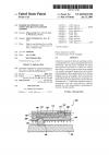
A method and apparatus for thermally conducting heat from a semiconductor device, namely, a flip-chip assembly. In one embodiment, a heat sink, such as a diamond layer having openings therein, is provided over a surface of a semiconductor device. Conductive pads are formed in the openings to be partially contacting the diamond layer and to electrically communicate with the semiconductor device. The heat produced from the semiconductor device and thermally conducting through the conductive pads i…
 
1 2 3 4 5 6 7 8 9 10
 
 
About |  FAQs |  Terms & Disclaimer |  Link to Us |  Contact Us